3dmid post-007
Update on 3D-MID
Ultrashort Pulse Laser
Laser structuring with subsequent metallization is one of the most common processes in the manufacture of 3D-MID parts. When it comes to laser structuring, a distinction is made between Laser Direct Structuring (LDS), Laser Subtractive Structuring (LSS), Laser Structuring – Chemical Activation (LS-ChA) and Photo-Chemical Structuring (Ph-Ch-S).
The above currently used processes follow different principals and each of them has its pros and cons. Most of these processes operate in the nano second range; however, there are some disadvantages associated with this. Ongoing developments show that the ultrashort pulse laser would be the better alternative for some of these processes.
In this article Waldemar Honstein, our laser specialist and one of the pioneers of LDS technology, will explain some interesting effects of laser structuring using Ultrashort pulse laser. I hope you enjoy reading it (kind regards/Nouhad)
Ultrashort pulse lasers in modern material processing
Ultra-short pulse lasers have become an indispensable part of modern material processing. Whether you are cutting, engraving or marking, you will find a selection of systems, that are using ultrashort pulse lasers, which can be applied to your application. Those new lasers open up new possibilities for effective material processing. Whether plastic or metal, glass or diamond materials, these can be structured by a pico- or femto-laser.
What is so special about the picosecond and femtosecond lasers?
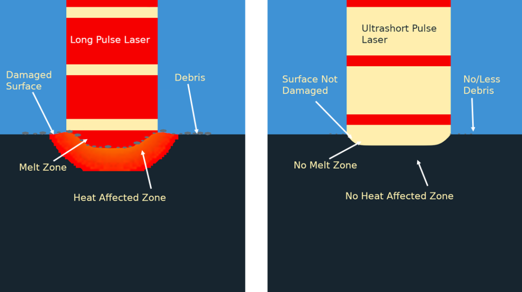
Regardless of what type of processing you use the laser for, traditional lasers heat the processed materials locally. Not only the processed area is thermally heated and modified in the process, but also adjacent areas. Depending on the application, to compensate for this, additional, complex processing steps may be necessary. In the worst case, if the thermal damage is inadmissible, instead of a laser process another, more expensive processing method must be utilized. Due to very short but high-energy pulses, the modification of the surface works with practically no heat input. Since there is no heat input, there is also no thermal damage to the adjacent areas and thus no reduction in the quality of the processed surfaces.
What is the benefit of using ultrashort pulse laser?
Analogous to other technologies, the advantages of an ultrashort pulse laser can also be advantageous for the 3D MID technology. Precise and clean structures on the substrate are crucial for quality and have an impact on subsequent processes. Here are some advantages of :
- Certain materials are sensitive to the input of heat. In order to avoid the thermal degradation of materials, processing parameters need to be adjusted accordingly, which usually results in longer processing times. With an ultrashort pulse laser there would not be such a restriction
- Thermal intake causes fraying edges of lasered surfaces. Ultrashort pulse lasers would create much cleaner edges here
- Drilling vias is a complex process because, on the one hand, the thermal input enables material to be removed and, on the other hand, the surrounding material must not be overheated. Achieving this balance usually results in long structuring times. A pico or femto laser would drastically reduce the processing time as well as improve the via quality.

3dmid post-006
New challenges require new solutions – 3D-MID for automotive applications
In the history of mankind there has been hardly any other technology that is causing such emotion and enthusiasm as the automobile. The car offers personal mobility and freedom that characterizes our way of life. While we get used to this freedom and we don’t want to give it up, yet we must deal with the negative side effects and keep the costs of this freedom as low as possible. This is a major challenge for car manufacturers.
Car manufacturer have taken on this challenge for a long time and have overcome a number of tasks. Significant reduction in CO2 emission was achieved in the last decade and countless safety and comfort options have been added. Plastics have replaced a large numbers of metal parts resulting in weight reduction, and electronics have found their way into automobiles to manage nearly everything in a car.
Driving assistance systems, for example, manage the distance to the vehicle in front, monitor the “blind spot”, warn the driver of unintentional lane departure, identify critical situations and help the driver to cope with them. These are just a few examples of the safety and convenience function of the modern automobile.
New challenges require new solutions
In order to work properly and safely these systems need to communicate with each other, and their integration requires space that shouldn’t come at the expense of user comfort. The diversity and complexity of these systems increases their fragility. This requires increased reliability and additional efforts to control such systems, and it is essential that the costs incurred must remain reasonable.
Reliable communication, space reduction and managing complexity at reasonable costs are significant challenges which must be taken into account while designing new products. In this regard 3D-MID technology can be of great help.
The advantages of 3D-MID technology
- Optimal use of space thanks to their three-dimensional shape
- Integration of mechanical and electronic functions by combining plastic and electronics
- Reduction in the number of components and process steps by integrating several components into a single module
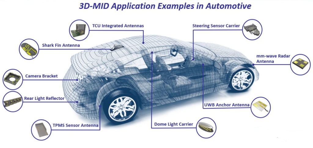
In other words, 3D-MID technology stands for miniaturization and system simplification. The technology already has a foothold in various industrial fields such as Medical, Electronics and Telecommunications. In recent years several hundreds of millions of 3D antennas for mobile phones have been manufactured. In the automotive field, 3D-MID is used for sensors, switches, antennas and more and more applications are being added.
Kind regards and best wishes
Nouhad
3dmid post-004
The semiconductor supply crisis
How to tackle the challenge of complexity?!

The bottleneck in semiconductor supply is currently on everyone’s lips. Sooner or later the crisis will surely be overcome, but this bottleneck indicates structural problems in the semiconductor industry that need to be addressed. Technically speaking, the manufacture of semiconductors is a highly complex process; In addition to the technical aspect of complexity, there is now also a political aspect. Things are so intertwined that they can no longer be separated or viewed separately. The value chain semiconductor graph shows how all countries in the world depends on one another to make semiconductors. China doesn’t seem to play a major role in the value chain at the moment, but it does when it comes to consumption of semiconductors. And China is making tremendous strides in terms of innovation and the shown graph can change very quickly.
How to master complexity?

So, with semiconductors we are dealing with a highly complex topic in every respect. When a system reaches a high degree of complexity that can only be mastered with greater complexity, then you must think about how you can simplify this system through intelligent solutions. Otherwise you will find yourself in a predicament of complexity with an unpredictable outcome. Is it possible to simplify a complex system without sacrificing performance, or possibly even to improve its performance by simplification? The answer is definitely – yes! An old example shows us that, namely the invention of the wheel.
Cooperation versus confrontation
The emerging protectionist tendencies in politics will not contribute to the solution of the complexity problems, rather the other way around, they will damage the own economy in the long run. Competition should be viewed as a positive component of business, not a threat. If you are sure of your abilities, why should you fear competition? The answer to the crisis should be cooperation instead of confrontation and simplification instead of more complexity. Politics should create the framework for an innovative market economy; science and industry should deal with simplifying complexity.
3D-MID as a simplified solution
There are good examples of how, for example, alternative simple solutions can be offered in comparison to highly complex wafer production. One of them shows a research study carried out by the Institute for Microproduction Technology at Leibniz Universität Hannover (IMPT) on the subject of manufacturing wafer substrates on a PEEK basis using the LDS process.
LDS is currently the most widespread 3D-MID process and offers many options, especially at the interface between the bare chips and the electronic circuits on the PCB. This interface currently offers greater potential for miniaturization than the chips themselves. For this, however, there are still some tasks to be mastered at the level of material and manufacturing processes. With increasing networking and digitization, as well as in industrial and consumer goods, there is no getting around miniaturizing these interfaces and simplifying them at the same time. 3D-MID can make a great, useful contribution here.
Link to the IMPT study: https://www.3d-mid.de/en/ensinger-lithography-free-production-of-sensors-and-microsystems/
Kind regards and best wishes
Nouhad
3dmid post-002